
Administrator
21 November 2024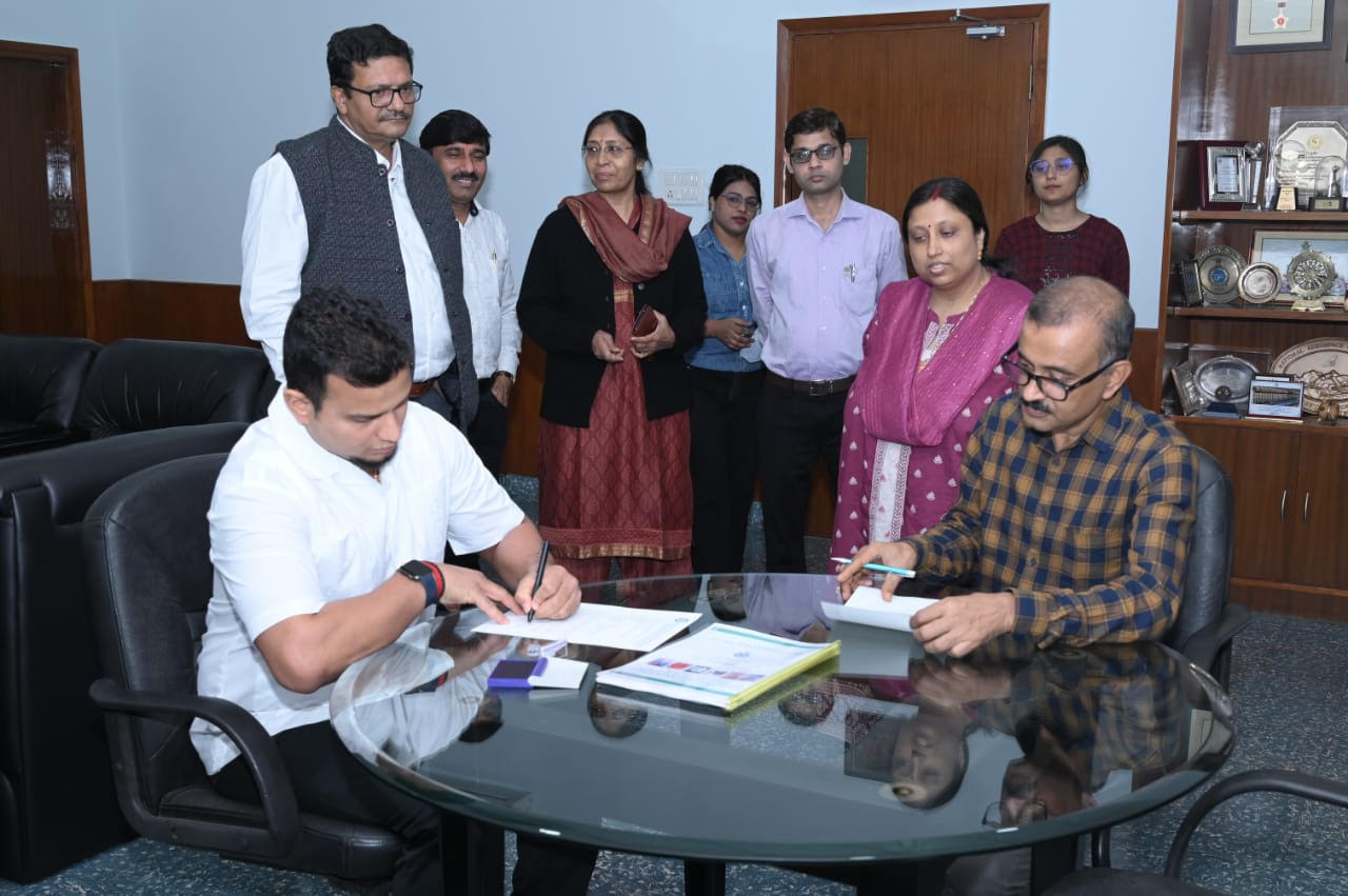
CSIR-NML, Jamshedpur,has announced the transfer of its innovative technology on waste printed circuit boards (PCBs) recycling to M/s Novasensa Pvt. Ltd., New Delhi on 21st November, 2024.
Over the years, CSIR-NML has successfully collaborated with numerous national and international industries and research organizations, fostering innovation and technological progress.
This milestone is part of CSIR-NML’s ongoing commitment to advancing sustainable technologies and promoting circular economies.
The recycling plant at Novasensa Pvt. Ltd., New Delhi, under the leadership of Mr. Aseem Trivedi, will harness this pioneering technology to process valuable metals and materials from waste PCBs.
The facility will operate with a focus on zero-waste principles, contributing significantly to society’s goal of sustainable development.
This environmentally friendly technology will enable the recovery of valuable metals and other materials which include mainly gold (Au), copper (Cu) and aluminum (Al) as metals/salts from waste PCBs, promoting electronic waste management and sustainable development.

The technology transfer was graced by a distinguished group of experts from CSIR-NML, including Dr. Sandip Ghosh Chowdhury, Director, CSIR-NML, Dr. Manis Kumar Jha, Project Leader, Dr. Sanjay Kumar, Head of MER, Dr. Jhumki Hait, Principal Scientist, Dr. Ranjeet Kr. Singh, Dr. Ankur Sharma, Dr. Krishna Kumar, Dr. S.K. Sahu, Mr. Shivendra Sinha, and a group of researchers, Dr. Rekha Panda, Ms. Rukshana Parween, Ms. Karina Rani and from the RPBD side, Dr. S.K. Pal and Dr. Beena Kumari.
The team was instrumental in completing the necessary documentation and formalizing the transfer of this innovative technology. Mr. Aseem Trivedi, Founder & CEO, M/s Novasensa Pvt. Ltd., New Delhi, expressed his enthusiasm about the new venture in e-waste recycling.
Mr. Aseem Trivedi said, “I am very excited to be part of this transformative initiative, bringing CSIR-NML’s PCBs recycling technology to the forefront of e-waste management in India. It is our goal to create a pollution-free society while ensuring the preservation of precious natural resources for future generations”.
Dr. Sandip Ghosh Chowdhury, Director, NML, Jamshedpur expressed his happiness and said, “In recent years, CSIR-NML has successfully transferred numerous indigenous technologies to Indian companies and hope that in future we will transfer more and more technologies to make India an e-waste free society”.
Waste PCBs will be recycled using NML's technology in Novasensa Pvt. Ltd., New Delhi The increasing generation of waste PCBs presents a significant environmental challenge, making their proper disposal and recycling crucial metals to prevent contamination from toxic substances and excessive metallic concentrations.
The unregulated and inefficient recycling of PCBs often leads to the loss of valuable metals and the release of harmful metals into the environment. The technology developed by NML, implemented at Novasensa Pvt. Ltd. in New Delhi, addresses this issue by offering an environmentally friendly solution for recovering metals such as gold (Au), copper (Cu), and aluminum (Al) from waste PCBs.
This approach not only reduces environmental pollution but also prevents the contamination of soil through industrial waste and sewage. The technology transfer process begins with the mechanical pre-treatment process of waste PCBs to obtain a metal concentrate, followed by leaching in appropriate lixiviants to extract metals into the leach liquor.
This is then purified using solvent extraction and evaporation/electro-winning techniques to recover high-purity metals and salts. The products i.e. metal/salts of Au, Cu and Al were extracted from the waste PCBs using a mechanical pre-treatment followed by hydro- and electro-metallurgical techniques.
The purity of the products was found very high i.e. salts >98.5% and metals >99.99%. Novelty of the present work lies in development of a simple feasible indigenous technology for Indian recycling company to recover Au, Cu and Al from the waste PCBs in an environmental friendly manner which is a newer concept for developing country like India The technology is indigenous, cost- effective and novel, providing a significant contribution to the advancement of science and technology, particularly in developing countries like India.
The PCBs recycling sector has note-worthy potential to contribute in country's economy and create employment. In the future, this technology could be scaled to small-scale industries and cottage industries, making it accessible to a broader segment of the population.
The process requires the use of chemical reagents, which is carried out under strict safety protocols, including the use of gloves, safety glasses, and masks to prevent health risks.
This innovation will raise awareness, new avenue/start-ups for new entrepreneurs and businesses in the field of waste recycling. Moreover, the technology has great potential to be adopted in various sectors viz., Government Industries, Municipal Sectors, Indian recycling industries, socio-economic organizations/ NGOs, Unemployed graduates, engineers, group of persons under co-operative, etc., contributing to both economic and social development.
The successful transfer of this environmentally- friendly technology is expected to significantly reduce the ecological footprint of e-waste while simultaneously recovering high-value metals, which are crucial in numerous industries. This process not only contributes to reducing pollution but also helps preserve vital natural resources for future generations.